Optimized for high-density edge deployments and enterprise access switches across Japan's leading industrial nodes.
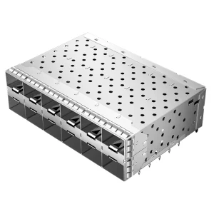
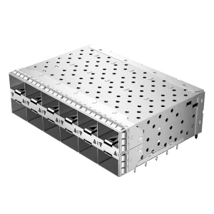
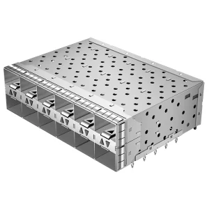
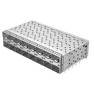
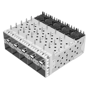
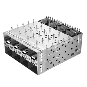
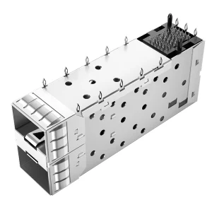
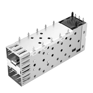
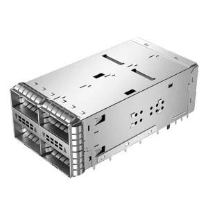
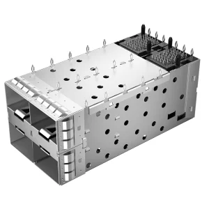
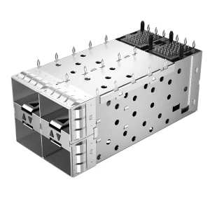
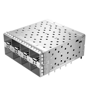
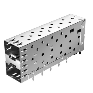
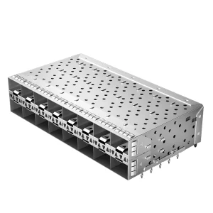
The acceleration of Japan’s digital economy—driven by ultra-low latency requirements in automated robotics, smart automotive lines in Nagoya, and the dense financial hubs of Tokyo and Osaka—has forced a major shift in modern networking hardware. Legacy single-row SFP cages are quickly being replaced by 2xN stacked port configurations (ranging from 2x1 and 2x2 to high-density 2x6 and 2x8 variants). This design effectively doubles the port density of host boards, allowing system hardware designers to maximize I/O throughput within standard 1RU form factors.
Japan’s unique manufacturing landscape mandates exceptionally strict adherence to spatial efficiency and strict safety parameters. Major telecoms like NT&T, KDDI, and SoftBank demand equipment that operates flawlessly under localized seismic events and elevated ambient thermal profiles. Consequently, selecting components sourced from factories with high-level signal integrity testing is no longer optional—it is a critical reliability requirement.
By leveraging advanced press-fit technology and integrated light pipes, OptiLinker’s 2xN solutions offer seamless replacements for legacy systems, supporting Japan's transition toward 25G and 56G PAM4 edge architectures.
Stacked architectures reduce the required footprint on PCBs by up to 50%, enabling high-density enterprise configurations. This is critical for space-constrained edge nodes in urban Japan.
Understanding the engineering challenges of multi-port stacked cages operating at 10Gbps to 28Gbps per channel.
Stacked modules naturally generate higher localized operating temperatures because the bottom row is shielded from typical airflow configurations. Incorporating custom light pipes and strategically placed ventilation holes ensures operating environments stay below 85°C.
High-speed lines generate electromagnetic radiation that can result in cross-channel noise. OptiLinker utilizes high-conductivity copper alloy shielding gaskets and multiple grounding fingers to satisfy VCCI Class A requirements in Japanese electronics.
Using press-fit (compliant pin) termination provides solderless, gas-tight electrical connections that stand up to structural vibrations and mechanical shifts, facilitating easy factory board reworking processes.
Our engineering utilizes advanced computational fluid dynamics (CFD) to model airflow profiles across stacked cages. This ensures that even under maximum 2.5W transceiver loads per port, temperature gradients are balanced across the top and bottom rows.
Engineered to support higher throughput profiles for industrial network interfaces.
Mitigating systemic risks in optical interconnect logistics for Japanese and global network equipment manufacturers.
Recent supply chain disruptions have driven global network infrastructure providers to reassess their dependency on single-source connector suppliers. For Japanese companies seeking high-density 2xN stacked SFP/SFP+ cages, local technical support and regional warehouse capabilities are key requirements. Procuring directly from qualified manufacturers like OptiLinker provides high-quality alternatives to standard TE, Molex, and Pulse components, reducing lead times from months to weeks.
Key global procurement considerations for stacked connector components include:
Ensure your optical hardware imports conform to localized regulatory frameworks:
1. VCCI Certification: Electromagnetic interference tests must conform to Class A/B requirements to prevent interference in high-density rack configurations.
2. Solder Quality Verification: Press-fit terminations should use standard compliant-pin (eye-of-the-needle) shapes to prevent damage to expensive PCB copper barrels during installation.
3. High-Quality Lead Alloys: OptiLinker ensures zero lead contamination across our production line to comply with RoHS regulations.
A professional optical transceiver manufacturer and solution provider specializing in high-speed optical communication modules.
Founded in 2016, OptiLinker operates a modern production facility under the brand name OptiLinker (www.optilinkertrans.com). With over 12 years of industry experience and approximately 8 years of export experience, we deliver engineered high-density transceiver and connector hardware for global datacenter and telecom applications.
Quality assurance is a core focus at OptiLinker. We implement 100% incoming material inspection, AOI automated optical inspection, and full optical performance testing. Product verification includes BER testing, eye diagram analysis, and high/low temperature cycling tests, ensuring stable performance under demanding network environments. Our engineering team specializes in high-speed optical design, signal integrity optimization, and protocol compatibility development.
OptiLinker offers flexible customization options including wavelength tuning, transmission distance, packaging form factors, firmware coding, and device compatibility programming. In the last year alone, OptiLinker launched approximately 120 new optical transceiver products, reflecting our continuous innovation and rapid response to market demand.
Our state-of-the-art production floors feature modern dust-free zones, automated micro-welding stations, and high-precision tooling systems designed specifically for advanced stacked ports assembly.
How next-generation physical interfaces will handle data rate scaling across Japanese networks.
As optical transceivers scale from 25G SFP28 and 100G QSFP28 to 400G and 800G structures, physical interconnect constraints become tighter. OptiLinker is developing next-generation cage and connector configurations designed to mitigate high-frequency loss.
High-frequency performance is critical for modern data routing. Next-generation designs feature improved pin geometry to minimize impedance mismatches at the connector-to-board transition zone, ensuring insertion loss remains minimal at high frequencies.
By routing optical fibres directly to on-board ASICs, CPO architectures bypass much of the electrical loss associated with traditional copper tracing. OptiLinker’s future roadmap includes hybrid connector solutions capable of accepting direct optical connections at the faceplate.
Answers to common technical questions asked by system hardware engineers and procurement managers.
A: Press-fit (compliant pin) cages provide solderless, gas-tight electrical connections that stand up to structural vibrations and mechanical shifts, facilitating easy factory board reworking processes. This makes them ideal for multi-layer PCBs used in high-end Japanese telecom nodes where thermal stress during wave soldering must be avoided.
A: Because stacked configurations (like 2x4, 2x6, 2x8) place transceivers on top of one another, the lower module has limited exposure to system-level airflow. OptiLinker cages address this by integrating dedicated air ducts, heat sinks, and light pipe designs to help maintain uniform operating temperatures across both rows.
A: Yes. Our cages are engineered to match standard industry footprints (e.g. 1-2007562-8, 2180640-1, 754625001), ensuring direct drop-in replacement options for existing PCB layouts without requiring design modifications.
A: Every production batch undergoes automated optical inspection (AOI) to verify pin geometry and assembly tolerances. We also perform insertion/extraction cycle tests, salt spray corrosion testing, and high-frequency signal integrity analysis (including BER testing and eye diagram verification) to ensure performance in demanding environments.
A: Yes. We offer flexible customization options, including different light pipe profiles (such as round, square, or flat shapes) and varying outer dimensions, to match the layout of your host board's LEDs.
Select from our range of high-performance connectors, fully compliant with international MSA standards.